Descrição do produto:
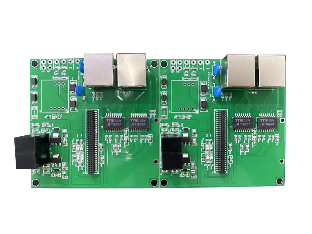
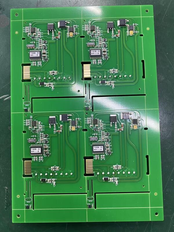
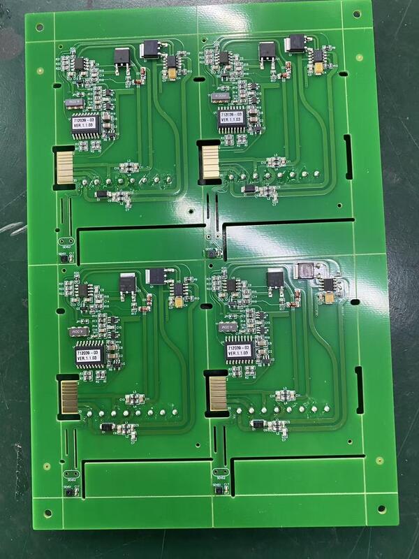
O conjunto de circuitos de circuito impresso de comunicação é uma solução altamente avançada e confiável concebida para satisfazer as exigências rigorosas dos sistemas de comunicação modernos.Este produto apresenta uma configuração PCB de 6 camadas sofisticada, o que garante uma excelente integridade do sinal, um melhor desempenho elétrico e uma resistência mecânica superior.O projeto multicamadas é essencial para acomodar layouts de circuitos complexos e componentes de alta densidade, tornando-o ideal para aplicações que exigem capacidades robustas de comunicação.
O núcleo deste conjunto de PCB de comunicação é a tecnologia de placa de PCB HDI (High-Density Interconnect).e maior densidade da plataforma de ligaçãoA utilização da tecnologia HDI neste conjunto permite uma maior funcionalidade em fatores de forma mais pequenos,permitir que os fabricantes produzam equipamentos de comunicação mais eficientes e compactos.
O controlo da impedância é uma característica crítica deste conjunto de PCB de comunicação, garantindo que a transmissão do sinal permaneça estável e livre de distorções em todos os planos.Impedância controlada é vital em circuitos de comunicação de alta frequência porque minimiza as reflexões do sinal e a intermitênciaEsta característica é especialmente importante para aplicações que envolvem transmissão de dados de alta velocidade e sinais RF sensíveis.quando a manutenção da integridade do sinal é primordial.
As opções de acabamento de superfície disponíveis para este produto incluem ENIG (Electroless Nickel Immersion Gold) e HASL (Hot Air Solder Leveling) Lead Free.Superfície soldável com excelente resistência à corrosão e longa vida útil, tornando-o altamente adequado para componentes de pitch fino e processos de montagem avançados.O acabamento sem chumbo HASL é uma opção ecológica que garante juntas de solda fiáveis e boa umedecibilidadeEstes acabamentos de superfície garantem que o conjunto de PCB de comunicação atenda a rigorosos padrões de qualidade e seja compatível com várias técnicas de montagem.
Outro atributo notável deste conjunto de PCB de comunicação é a diversidade de tipos via incorporados em seu design.que, em conjunto, aumentam o desempenho elétrico e a flexibilidade de roteamento do PCBAs vias de buraco passam inteiramente através da placa, as vias cegas ligam as camadas externas a uma ou mais camadas internas sem atravessar toda a placa e as vias enterradas ligam apenas as camadas internas.Esta variedade de tipos via permite otimizar os caminhos de sinal, redução da indutividade parasitária e aumento da densidade dos componentes, todos os quais contribuem para um desempenho superior de comunicação.
Este conjunto de PCB de comunicação é fabricado por um fabricante respeitável conhecido pelo seu compromisso com a qualidade, precisão e inovação.O fabricante utiliza técnicas de fabrico de ponta e medidas de controlo de qualidade rigorosas para garantir que cada conjunto de PCB cumpra os mais elevados padrões da indústria.Uma das principais características oferecidas por este fabricante é a inclusão de camadas grossas de cobre dentro da empilha de PCB.Melhora a gestão térmica, e aumenta a durabilidade geral do conjunto, o que torna o conjunto de PCB de comunicação particularmente adequado para dispositivos de comunicação que consomem muita energia e ambientes operacionais exigentes.
Em resumo, a Communication PCB Assembly destaca-se como um produto de primeira linha que combina tecnologia avançada de PCB HDI, construção de 6 camadas, controle de impedância preciso, versatilidade através de tipos,e opções de acabamento de superfície premium como ENIG e HASL livre de chumboCom a integração de cobre grosso e a habilidade especializada do fabricante, este conjunto oferece desempenho elétrico excepcional, robustez mecânica e fiabilidade a longo prazo. It is an ideal choice for manufacturers and developers aiming to build cutting-edge communication equipment that requires superior PCB assemblies capable of handling complex signals and stringent environmental conditions.
Características:
- Nome do produto: Reunião de PCB de comunicação
- Especificação: PCB de tamanho personalizado
- Revestimento de superfície: ENIG, HASL livre de chumbo
- Controle da impedância: Sim
- Sistema de qualidade de PCB: conforme com a ROHS
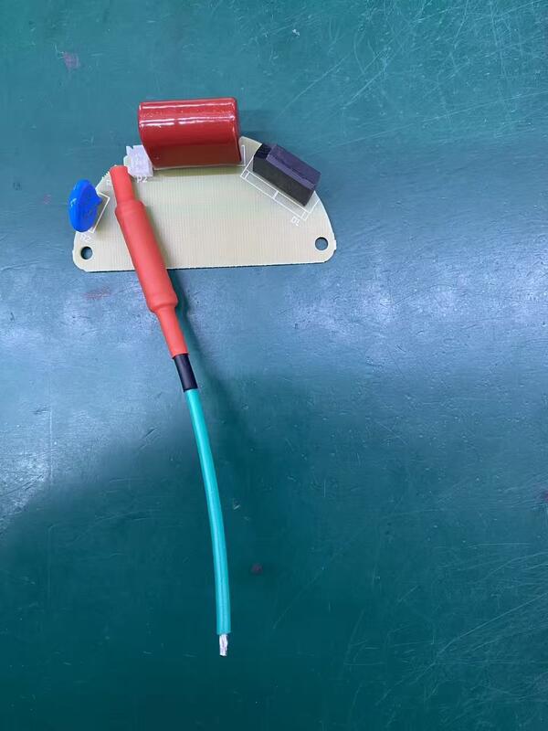
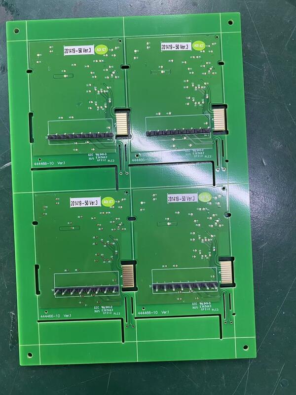
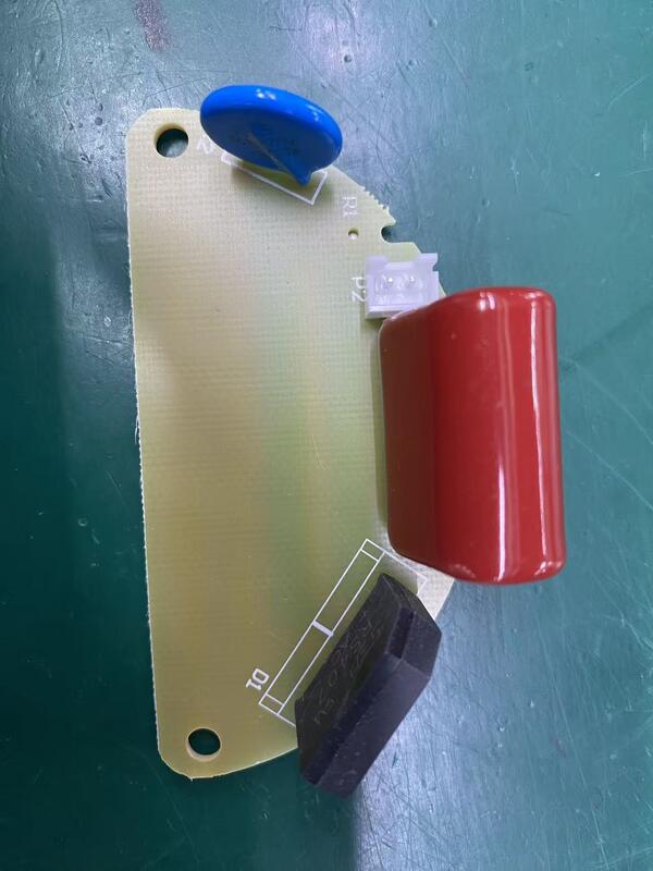
- Viatype: Através do Buraco, Cego, Enterrado
- Projetado por um fabricante de confiança especializado em conjuntos de PCB de alta qualidade
- Características de protecção contra sobretensões reforçadas para garantir um desempenho de comunicação fiável
- Mecanismos avançados de protecção contra sobretensões integrados para uma segurança óptima do circuito
Parâmetros técnicos:
| Nome do produto |
Assemblagem de PCB de comunicação |
| Camadas de PCB |
6 Camadas |
| Área de aplicação |
Comunicação 5G, Infraestrutura de Comunicação |
| Controle da impedância |
- Sim, sim. |
| Especificações |
Tamanho de PCB personalizado |
| Cor da máscara de solda |
Azul, verde, etc. |
| Placas de PCB |
HDI PCB |
| Personalizado |
- Sim, sim. |
| PCB de comunicação |
Alto Tg170 e Alto Tg180 |
| Sistema de qualidade de PCB |
ROHS |
| Características especiais |
O cobre espesso para uma infraestrutura de comunicação melhorada |
Aplicações:
A Assembleia de PCB de Comunicação, com 6 camadas e avançada através de tipos incluindo vias Through Hole, Blind e Buried, é um componente essencial no campo da comunicação 5G em rápida evolução.Este produto foi meticulosamente concebido e fabricado para satisfazer as exigências de alto desempenho dos sistemas de comunicação modernosComo uma solução de PCB personalizada, oferece flexibilidade em tamanho e especificações,permitir que os fabricantes adaptem a placa aos requisitos específicos do dispositivo e aos cenários de aplicação.
Uma das principais ocasiões de aplicação para esta montagem de PCB de comunicação é em equipamentos de infraestrutura 5G, como estações base, repetidores de sinal e roteadores de rede.As espessas camadas de cobre incorporadas no projeto proporcionam excelente capacidade de carga de corrente e gestão térmica, que são críticos para lidar com os sinais de alta frequência e os níveis de potência típicos do hardware de comunicação 5G.Isto torna o produto particularmente adequado para ambientes exteriores e industriais onde a durabilidade e o desempenho consistente são primordiais.
Além disso, este conjunto de PCB é amplamente utilizado em dispositivos de comunicação que exigem placas de circuito compactas, mas altamente eficientes.permite uma maior densidade de circuito e uma melhor compatibilidade eletromagnéticaIsto é crucial em dispositivos de comunicação móvel, gateways IoT e módulos de comunicação sem fio onde as restrições de espaço e a integridade do sinal são considerações significativas.Os fabricantes beneficiam das opções de tamanho personalizadas, permitindo-lhes integrar o PCB sem problemas em várias arquiteturas de dispositivos.
Além disso, o conjunto de PCB de comunicação é utilizado em equipamentos de ensaio e medição em laboratórios de telecomunicações.Os processos de fabricação de precisão garantem qualidade e desempenho consistentes, que são essenciais para testes precisos de sinais e dispositivos de comunicação 5G. Os fabricantes dependem destes PCBs para criar protótipos e desenvolver novas tecnologias de comunicação,Aproveitamento dos recursos personalizáveis e do design robusto para acelerar os ciclos de inovação.
No geral, este produto constitui uma pedra angular do ecossistema de comunicação 5G, preenchendo a lacuna entre o design eletrónico avançado e as necessidades de aplicação prática.Os fabricantes valorizam suas camadas de cobre espessas e versátil através de opções para criar confiável, soluções de comunicação de alto desempenho adaptadas a cenários diversos, desde infra-estruturas de rede de grande escala até dispositivos de comunicação portáteis e compactos.
Personalização:
Nosso produto de montagem de PCB de comunicação oferece serviços de personalização excepcionais adaptados para atender às suas necessidades específicas.Estes PCB garantem uma estabilidade térmica e fiabilidade superiores para aplicações exigentesFornecemos opções de tamanho de PCB personalizado para se adequar perfeitamente aos seus requisitos de design, tornando-o ideal para sistemas avançados de comunicação 5G.
Com um controlo de impedância preciso, os nossos PCBs garantem uma integridade óptima do sinal e um desempenho crítico para dispositivos de comunicação de alta frequência.Aumentar a capacidade de carga da corrente e permitir aplicações de corrente pesada sem comprometer a durabilidadeO nosso compromisso com a qualidade é demonstrado pela adesão ao padrão ROHS, garantindo produtos ecológicos e seguros.
Escolha nossos serviços de montagem de PCB de comunicação para PCBs robustos e de alto desempenho que se destacam em ambientes de comunicação 5G,Oferecendo construção de cobre grosso e capacidades de manuseio de corrente pesada personalizadas para suas especificações.
Apoio e Serviços:
Nosso produto de montagem de PCB de comunicação é apoiado por um suporte técnico e serviços abrangentes para garantir desempenho e confiabilidade ideais.Fornecemos assistência especializada durante todo o ciclo de vida do produto, desde a consultoria de projeto e desenvolvimento de protótipos até à produção e apoio pós-venda.
Nossa equipe de suporte técnico está disponível para ajudar a resolver qualquer problema, oferecer orientação sobre integração e compatibilidade e fornecer documentação e recursos detalhados.Também oferecemos serviços de personalização para atender aos requisitos específicos da aplicação e garantir uma comunicação contínua dentro dos seus sistemas.
Com foco na garantia de qualidade, os nossos serviços incluem processos rigorosos de ensaios e inspecções para garantir os mais elevados padrões de desempenho e durabilidade.Estamos comprometidos em fornecer soluções oportunas e melhorias contínuas para melhorar sua experiência com nossos produtos de montagem de PCB de comunicação.
Faça parceria conosco para obter suporte técnico confiável e serviços personalizados que permitam que seus projetos de tecnologia de comunicação tenham sucesso.
Embalagem e transporte:
Os nossos produtos de montagem de PCB de comunicação são meticulosamente embalados para garantir a máxima proteção durante o transporte.Cada conjunto de PCB é colocado com segurança em sacos anti-estáticos para evitar danos por descarga eletrostáticaEstes são então amortecidos com espuma ou borracha para absorver choques e vibrações.
Os conjuntos embalados são colocados em caixas de cartão ondulado de parede dupla e resistentes, concebidas para suportar manipulação áspera e fatores ambientais.paletes e caixas personalizados são utilizados para facilitar o transporte seguro.
Empregamos parceiros de transporte confiáveis e fornecemos informações de rastreamento para garantir a entrega atempada e segura.Todas as remessas cumprem as normas e regulamentos internacionais de transporte marítimo para garantir a integridade do produto à chegada.


 Por favor verifique seu email!